Global EUV Lithography Market Set to Expand at 21.5% CAGR, Surpassing USD 22,978.6 Million by 2029 | FMI Reports
Posted on 2024-09-06 by Future Market Insights in Industrial // 0 Comments
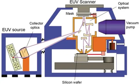
In 2021, global sales in the EUV (Extreme Ultraviolet) lithography market were estimated at USD 4,648.6 million. Looking ahead to 2029, the market is anticipated to grow significantly, with a projected compound annual growth rate (CAGR) of 21.5%, reaching an estimated value of USD 22,978.6 million. EUV lithography uses a specific wavelength of light to create advanced semiconductor components, and the development of more sophisticated lithographic systems is a key driver behind its adoption.
The EUV Lithography Market report by Future Market Insights—an ESOMAR Certified Market Research and Consulting Firm—offers comprehensive insights and analysis of the EUV lithography sector. This report provides detailed information on market drivers, size, forecasts, revenue, and shipment segmentations, along with a ten-year outlook through 2029. It also evaluates major industry players, competitive dynamics, and regional trends.
The EUV lithography market is poised for substantial growth, fueled by the ongoing push for miniaturization of integrated circuits and microchips, rising demand for higher wafer production, and the expanding semiconductor industry. As technology advances to improve performance and efficiency, EUV lithography is becoming essential for achieving the high resolution required for advanced semiconductor manufacturing processes.
This advanced technology enables the precise creation of complex patterns on silicon wafers, facilitating the production of smaller, faster, and more powerful semiconductors. The integration of EUV lithography is closely linked to the miniaturization of integrated circuits, increased wafer production scales, and the robust growth of the semiconductor industry.
Despite its promising future, the adoption of EUV lithography in chip manufacturing is currently cautious due to the technology’s nascent stage and high upfront costs. However, ongoing innovation and research and development are expected to make EUV lithography more efficient and cost-effective, driving its broader adoption in the coming years.
Full Market Assessment: Comprehensive Report
Key Takeaways:
- Reduction of microchip sizes to incorporate them into shrinking semiconductors is one of the prime factors that resulted in the development of EUV lithography technology.
- Emergence of artificial intelligence (AI), machine learning, industrial IoT (IIoT), and autonomous driving has been driving miniaturization of microchips, subsequently creating the need for EUV lithography in chip manufacturing.
- Constant innovation, R&D, and retrofitting of installed systems to improve wafer production, are anticipated to remain key trends in the EUV lithography market.
- Integrated device manufacturers (IDM) and foundries are projected to create bulk of the demand for EUV lithography systems, as they are responsible for majority of the microchip and integrated circuit (IC) demand across industries.
- Acquisition of stakes in key technology-based companies to complement product development is anticipated to remain a prominent trend in the market.
Competitive Landscape
Key players in the EUV Lithography market are focusing on a data-centric approach with an aim of expanding their portfolio of technology solutions that address customer needs. Many key players are also using innovation to expand their product offerings to meet customer requirements. Players are aiming at research & development to develop new products.
For Instance:
- In Jan 2022, ASML and Intel Corporation announced the latest phase of their longstanding collaboration to advance cutting-edge semiconductor lithography technology.
- In April 2019, Taiwan Semiconductor Manufacturing Co. Ltd announced the expansion of the Open Innovation Platform ® (OIP) Cloud Alliance, with Mentor Graphics joining inaugural members Amazon Web Services, Cadence, Microsoft Azure, and Synopsys.
- In March 2019, Samsung Electronics developed a 3rd-generation 10-nanometer-class (1z-nm) eight-gigabit (GB) Double Data Rate 4 (DDR4) DRAM for the first time in the industry.
- In October 2019, SK Hynix developed 1Znm 16GB (Gigabits) DDR4 (Double Data Rate 4) DRAM. As 16 GB is the industry’s largest density for a single chip, the total memory capacity per wafer is also the largest of the existing DRAMs.
Key Players
- ASML
- Nikon
- Canon
- Carl Zeiss
- Toppan Printing
- NTT Advanced Technology
- Intel
- Samsung
- SK Hynix
- Toshiba
- TSMC
- Global Foundries
Global EUV Lithography Market by Category By End Use :
- Integrated Device Manufacturer (IDM)
- Foundry
- Memory
By Region:
- Americas
- EMEA
- Asia Pacific
About Future Market Insights (FMI)
Future Market Insights, Inc. (ESOMAR certified, recipient of the Stevie Award, and a member of the Greater New York Chamber of Commerce) offers profound insights into the driving factors that are boosting demand in the market. FMI stands as the leading global provider of market intelligence, advisory services, consulting, and events for the Packaging, Food and Beverage, Consumer Technology, Healthcare, Industrial, and Chemicals markets. With a vast team of 400 analysts worldwide, FMI provides global, regional, and local expertise on diverse domains and industry trends across more than 110 countries.
Contact Us:
Future Market Insights Inc.
Christiana Corporate, 200 Continental Drive,
Suite 401, Newark, Delaware – 19713, USA
T: +1-845-579-5705
For Sales Enquiries: sales@futuremarketinsights.com
Website: https://www.futuremarketinsights.com
LinkedIn| Twitter| Blogs | YouTube
Matched content
Editor’s pick
- Digi Communications N.V. announces that a share transaction was made by a Non-Executive Director of the Company with class B shares
- La Ballata del Trasimeno: Il Mediometraggio si Trasforma in Mini Serie
- Digi Communications NV Announces Availability of 2024 Preliminary Financial Report
- Digi Communications N.V. announces the recent evolution and performance of the Company’s subsidiary in Spain
- BevZero Equipment Sales and Distribution Enhances Dealcoholization Capabilities with New ClearAlc 300 l/h Demonstration Unit in Spain Facility
- Digi Communications NV announces Investors Call for the presentation of the 2024 Preliminary Financial Results
- Reuters webinar: Omnibus regulation Reuters post-analysis
- Patients as Partners® Europe Launches the 9th Annual Event with 2025 Keynotes, Featured Speakers and Topics
- eVTOLUTION: Pioneering the Future of Urban Air Mobility
- Reuters webinar: Effective Sustainability Data Governance
- Las acusaciones de fraude contra Ricardo Salinas no son nuevas: una perspectiva histórica sobre los problemas legales del multimillonario
- Digi Communications N.V. Announces the release of the Financial Calendar for 2025
- USA Court Lambasts Ricardo Salinas Pliego For Contempt Of Court Order
- 3D Electronics: A New Frontier of Product Differentiation, Thinks IDTechEx
- Ringier Axel Springer Polska Faces Lawsuit for Over PLN 54 million
- Digi Communications N.V. announces the availability of the report on corporate income tax information for the financial year ending December 31, 2023
- Unlocking the Multi-Million-Dollar Opportunities in Quantum Computing
- Digi Communications N.V. Announces the Conclusion of Facilities Agreements by Companies within Digi Group
- The Hidden Gem of Deep Plane Facelifts
- KAZANU: Redefining Naturist Hospitality in Saint Martin
- Enjoy Up to 35% Off MovPilot Video Downloaders this Black Friday
- New IDTechEx Report Predicts Regulatory Shifts Will Transform the Electric Light Commercial Vehicle Market
- Almost 1 in 4 Planes Sold in 2045 to be Battery Electric, Finds IDTechEx Sustainable Aviation Market Report
- Up to 50% Off TuneFab Music Converters with Coupon Code 2024
- Digi Communications N.V. announces the release of Q3 2024 financial results
- Digi Communications NV announces Investors Call for the presentation of the Q3 2024 Financial Results
- Pilot and Electriq Global announce collaboration to explore deployment of proprietary hydrogen transport, storage and power generation technology
- Digi Communications N.V. announces the conclusion of a Memorandum of Understanding by its subsidiary in Romania
- Digi Communications N.V. announces that the Company’s Portuguese subsidiary finalised the transaction with LORCA JVCO Limited
- Richard Reid Partners with Goodspace Anxiety Aid In Support of International Men’s Day
- Digi Communications N.V. announces that the Portuguese Competition Authority has granted clearance for the share purchase agreement concluded by the Company’s subsidiary in Portugal
- OMRON Healthcare introduceert nieuwe bloeddrukmeters met AI-aangedreven AFib-detectietechnologie; lancering in Europa september 2024
- OMRON Healthcare dévoile de nouveaux tensiomètres dotés d’une technologie de détection de la fibrillation auriculaire alimentée par l’IA, lancés en Europe en septembre 2024
- OMRON Healthcare presenta i nuovi misuratori della pressione sanguigna con tecnologia di rilevamento della fibrillazione atriale (AFib) basata sull’IA, in arrivo in Europa a settembre 2024
- OMRON Healthcare presenta los nuevos tensiómetros con tecnología de detección de fibrilación auricular (FA) e inteligencia artificial (IA), que se lanzarán en Europa en septiembre de 2024
- Alegerile din Moldova din 2024: O Bătălie pentru Democrație Împotriva Dezinformării
- Northcrest Developments launches design competition to reimagine 2-km former airport Runway into a vibrant pedestrianized corridor, shaping a new era of placemaking on an international scale
- The Road to Sustainable Electric Motors for EVs: IDTechEx Analyzes Key Factors
- Infrared Technology Breakthroughs Paving the Way for a US$500 Million Market, Says IDTechEx Report
- MegaFair Revolutionizes the iGaming Industry with Skill-Based Games
- European Commission Evaluates Poland’s Media Adherence to the Right to be Forgotten
- Global Race for Autonomous Trucks: Europe a Critical Region Transport Transformation
- Top Performing Investment Manager, Chetan Kapur of ThinkStrategy Capital Management, Went Way Above and Beyond for Investors which Enjoyed Leading Returns for over a Decade. Chetan Kapur Gets Unjustly and Unjustifiably Persecuted by the Corrupt, Racist and Power Abusing Element at the Securities and Exchange Commission
- Digi Communications N.V. confirms the full redemption of €450,000,000 Senior Secured Notes
- AT&T Obtiene Sentencia Contra Grupo Salinas Telecom, Propiedad de Ricardo Salinas, Sus Abogados se Retiran Mientras Él Mueve Activos Fuera de EE.UU. para Evitar Pagar la Sentencia
- Global Outlook for the Challenging Autonomous Bus and Roboshuttle Markets
- Evolving Brain-Computer Interface Market More Than Just Elon Musk’s Neuralink, Reports IDTechEx
- Latin Trails Wraps Up a Successful 3rd Quarter with Prestigious LATA Sustainability Award and Expands Conservation Initiatives
- Astor Asset Management 3 Ltd leitet Untersuchung für potenzielle Sammelklage gegen Ricardo Benjamín Salinas Pliego von Grupo ELEKTRA wegen Marktmanipulation und Wertpapierbetrug ein
- Digi Communications N.V. announces that the Company’s Romanian subsidiary exercised its right to redeem the Senior Secured Notes due in 2025 in principal amount of €450,000,000
- Astor Asset Management 3 Ltd Inicia Investigación de Demanda Colectiva Contra Ricardo Benjamín Salinas Pliego de Grupo ELEKTRA por Manipulación de Acciones y Fraude en Valores
- Astor Asset Management 3 Ltd Initiating Class Action Lawsuit Inquiry Against Ricardo Benjamín Salinas Pliego of Grupo ELEKTRA for Stock Manipulation & Securities Fraud
- Digi Communications N.V. announced that its Spanish subsidiary, Digi Spain Telecom S.L.U., has completed the first stage of selling a Fibre-to-the-Home (FTTH) network in 12 Spanish provinces
- Natural Cotton Color lancia la collezione "Calunga" a Milano
- Astor Asset Management 3 Ltd: Salinas Pliego Incumple Préstamo de $110 Millones USD y Viola Regulaciones Mexicanas
- Astor Asset Management 3 Ltd: Salinas Pliego Verstößt gegen Darlehensvertrag über 110 Mio. USD und Mexikanische Wertpapiergesetze
- ChargeEuropa zamyka rundę finansowania, której przewodził fundusz Shift4Good tym samym dokonując historycznej francuskiej inwestycji w polski sektor elektromobilności
- Strengthening EU Protections: Robert Szustkowski calls for safeguarding EU citizens’ rights to dignity
- Digi Communications NV announces the release of H1 2024 Financial Results
- Digi Communications N.V. announces that conditional stock options were granted to a director of the Company’s Romanian Subsidiary
- Digi Communications N.V. announces Investors Call for the presentation of the H1 2024 Financial Results
- Digi Communications N.V. announces the conclusion of a share purchase agreement by its subsidiary in Portugal
- Digi Communications N.V. Announces Rating Assigned by Fitch Ratings to Digi Communications N.V.
- Digi Communications N.V. announces significant agreements concluded by the Company’s subsidiaries in Spain
- SGW Global Appoints Telcomdis as the Official European Distributor for Motorola Nursery and Motorola Sound Products
- Digi Communications N.V. announces the availability of the instruction regarding the payment of share dividend for the 2023 financial year
- Digi Communications N.V. announces the exercise of conditional share options by the executive directors of the Company, for the year 2023, as approved by the Company’s Ordinary General Shareholders’ Meetings from 18th May 2021 and 28th December 2022
- Digi Communications N.V. announces the OGMS resolutions and the availability of the approved 2023 Annual Report
- Czech Composer Tatiana Mikova Presents Her String Quartet ‘In Modo Lidico’ at Carnegie Hall
- Discover the wonders of Masai Mara with Cruzeiro Safaris Kenya. Join our local tours and trips from Nairobi for an unforgettable experience
- SWIFTT: A Copernicus-based forest management tool to map, mitigate, and prevent the main threats to EU forests
- WickedBet Unveils Exciting Euro 2024 Promotion with Boosted Odds
- Museum of Unrest: a new space for activism, art and design
- Digi Communications N.V. announces the conclusion of a Senior Facility Agreement by companies within Digi Group
- Digi Communications N.V. announces the agreements concluded by Digi Romania (formerly named RCS & RDS S.A.), the Romanian subsidiary of the Company
- Top Performing Investment Manager, Chetan Kapur of ThinkStrategy Capital Management, Went Way Above and Beyond for Investors which Enjoyed Leading Returns for over a Decade. Chetan Kapur Gets Unjustly and Unjustifiably Persecuted by the Corrupt, Racist and Power Abusing Element at the Securities and Exchange Commission
- Green Light for Henri Hotel, Restaurants and Shops in the “Alter Fischereihafen” (Old Fishing Port) in Cuxhaven, opening Summer 2026
- Digi Communications N.V. reports consolidated revenues and other income of EUR 447 million, adjusted EBITDA (excluding IFRS 16) of EUR 140 million for Q1 2024
- Digi Communications announces the conclusion of Facilities Agreements by companies from Digi Group
- Digi Communications N.V. Announces the convocation of the Company’s general shareholders meeting for 25 June 2024 for the approval of, among others, the 2023 Annual Report
- Digi Communications NV announces Investors Call for the presentation of the Q1 2024 Financial Results
- Digi Communications intends to propose to shareholders the distribution of dividends for the fiscal year 2023 at the upcoming General Meeting of Shareholders, which shall take place in June 2024
- Digi Communications N.V. announces the availability of the Romanian version of the 2023 Annual Report
- Digi Communications N.V. announces the availability of the 2023 Annual Report
- International Airlines Group adopts Airline Economics by Skailark ↗️
- BevZero Spain Enhances Sustainability Efforts with Installation of Solar Panels at Production Facility
- Digi Communications N.V. announces share transaction made by an Executive Director of the Company with class B shares
- BevZero South Africa Achieves FSSC 22000 Food Safety Certification
- Digi Communications N.V.: Digi Spain Enters Agreement to Sell FTTH Network to International Investors for Up to EUR 750 Million
- Patients as Partners® Europe Announces the Launch of 8th Annual Meeting with 2024 Keynotes and Topics
- driveMybox continues its international expansion: Hungary as a new strategic location
- Monesave introduces Socialised budgeting: Meet the app quietly revolutionising how users budget
- Digi Communications NV announces the release of the 2023 Preliminary Financial Results
- Digi Communications NV announces Investors Call for the presentation of the 2023 Preliminary Financial Results
- Lensa, един от най-ценените търговци на оптика в Румъния, пристига в България. Първият шоурум е открит в София
- Criando o futuro: desenvolvimento da AENO no mercado de consumo em Portugal
- Digi Communications N.V. Announces the release of the Financial Calendar for 2024
- Customer Data Platform Industry Attracts New Participants: CDP Institute Report
- eCarsTrade annonce Dirk Van Roost au poste de Directeur Administratif et Financier: une décision stratégique pour la croissance à venir
- BevZero Announces Strategic Partnership with TOMSA Desil to Distribute equipment for sustainability in the wine industry, as well as the development of Next-Gen Dealcoholization technology
- Digi Communications N.V. announces share transaction made by a Non-Executive Director of the Company with class B shares
- Digi Spain Telecom, the subsidiary of Digi Communications NV in Spain, has concluded a spectrum transfer agreement for the purchase of spectrum licenses
- Эксперт по торговле акциями Сергей Левин запускает онлайн-мастер-класс по торговле сырьевыми товарами и хеджированию
- Digi Communications N.V. announces the conclusion by Company’s Portuguese subsidiary of a framework agreement for spectrum usage rights
- North Texas Couple Completes Dream Purchase of Ouray’s Iconic Beaumont Hotel
- Предприниматель и филантроп Михаил Пелег подчеркнул важность саммита ООН по Целям устойчивого развития 2023 года в Нью-Йорке
- Digi Communications NV announces the release of the Q3 2023 Financial Results
- IQ Biozoom Innovates Non-Invasive Self-Testing, Empowering People to Self-Monitor with Laboratory Precision at Home
- BevZero Introduces Energy Saving Tank Insulation System to Europe under name “BevClad”
- Motorvision Group reduces localization costs using AI dubbing thanks to partnering with Dubformer
- Digi Communications NV Announces Investors Call for the Q3 2023 Financial Results
- Jifiti Granted Electronic Money Institution (EMI) License in Europe
- Предприниматель Михаил Пелег выступил в защиту образования и грамотности на мероприятии ЮНЕСКО, посвящённом Международному дню грамотности
- VRG Components Welcomes New Austrian Independent Agent
- Digi Communications N.V. announces that Digi Spain Telecom S.L.U., its subsidiary in Spain, and abrdn plc have completed the first investment within the transaction having as subject matter the financing of the roll out of a Fibre-to-the-Home (“FTTH”) network in Andalusia, Spain
- Продюсер Михаил Пелег, как сообщается, работает над новым сериалом с участием крупной голливудской актрисы
- Double digit growth in global hospitality industry for Q4 2023
- ITC Deploys Traffic Management Solution in Peachtree Corners, Launches into United States Market
- Cyviz onthult nieuwe TEMPEST dynamische controlekamer in Benelux, Nederland
- EU-Funded CommuniCity Launches its Second Open Call
- Astrologia pode dar pistas sobre a separação de Sophie Turner e Joe Jonas
- La astrología puede señalar las razones de la separación de Sophie Turner y Joe Jonas
- Empowering Europe against infectious diseases: innovative framework to tackle climate-driven health risks
- Montachem International Enters Compostable Materials Market with Seaweed Resins Company Loliware
- Digi Communications N.V. announces that its Belgian affiliated companies are moving ahead with their operations
- Digi Communications N.V. announces the exercise of conditional share options by an executive director of the Company, for the year 2022, as approved by the Company’s Ordinary General Shareholders’ Meeting from 18 May 2021
- Digi Communications N.V. announces the availability of the instruction regarding the payment of share dividend for the 2022 financial year
- Digi Communications N.V. announces the availability of the 2022 Annual Report
- Русские эмигранты усиливают призывы «Я хочу, чтобы вы жили» через искусство
- BevZero Introduces State-of-the-Art Mobile Flash Pasteurization Unit to Enhance Non-Alcoholic Beverage Stability at South Africa Facility
- Russian Emigrés Amplify Pleas of “I Want You to Live” through Art
- Digi Communications NV announces the release of H1 2023 Financial Results
- Digi Communications NV Announces Investors Call for the H1 2023 Financial Results
- Digi Communications N.V. announces the convocation of the Company’s general shareholders meeting for 18 August 2023 for the approval of, among others, the 2022 Annual Report
- “Art Is Our Weapon”: Artists in Exile Deploy Their Talents in Support of Peace, Justice for Ukraine
- Digi Communications N.V. announces the availability of the 2022 Annual Financial Report
- “AmsEindShuttle” nuevo servicio de transporte que conecta el aeropuerto de Eindhoven y Ámsterdam
- Un nuovo servizio navetta “AmsEindShuttle” collega l’aeroporto di Eindhoven ad Amsterdam
- Digi Communications N.V. announces the conclusion of an amendment agreement to the Facility Agreement dated 26 July 2021, by the Company’s Spanish subsidiary
- Digi Communications N.V. announces an amendment of the Company’s 2023 financial calendar
- iGulu F1: Brewing Evolution Unleashed
- Почему интерактивная «Карта мира» собрала ключевые антивоенные сообщества россиян по всему миру и становится для них важнейшим инструментом
- Hajj Minister meets EU ambassadors to Saudi Arabia
- Online Organizing Platform “Map of Peace” Emerges as Key Tool for Diaspora Activists
- Digi Communications N.V. announces that conditional stock options were granted to executive directors of the Company based on the general shareholders’ meeting approval from 18 May 2021
- Digi Communications N.V. announces the release of the Q1 2023 financial results
- AMBROSIA – A MULTIPLEXED PLASMO-PHOTONIC BIOSENSING PLATFORM FOR RAPID AND INTELLIGENT SEPSIS DIAGNOSIS AT THE POINT-OF-CARE
- Digi Communications NV announces Investors Call for the Q1 2023 Financial Results presentation
- Digi Communications N.V. announces the amendment of the Company’s 2023 financial calendar
- Digi Communications N.V. announces the conclusion of two Facilities Agreements by the Company’s Romanian subsidiary
- Digi Communications N.V. announces the conclusion of a Senior Facility Agreement by the Company’s Romanian subsidiary
- Africa Luxury Trips, Luxury Accommodations, Tours, Excursions, Attractions and Vacation Holidays in Nairobi, Kenya
- Patients as Partners Europe Returns to London and Announces Agenda Highlights
- GRETE PROJECT RESULTS PRESENTED TO TEXTILE INDUSTRY STAKEHOLDERS AT INTERNATIONAL CELLULOSE FIBRES CONFERENCE
- Digi Communications N.V. announces Digi Spain Telecom S.L.U., its subsidiary in Spain, entered into an investment agreement with abrdn to finance the roll out of a Fibre-to-the-Home (FTTH) network in Andalusia, Spain
- XSpline SPA / University of Linz (Austria): the first patient has been enrolled in the international multicenter clinical study for the Cardiac Resynchronization Therapy DeliveRy guided by non-Invasive electrical and VEnous anatomy assessment (CRT-DRIVE)
- Franklin Junction Expands Host Kitchen® Network To Europe with Digital Food Hall Pioneer Casper
- Unihertz a dévoilé un nouveau smartphone distinctif, Luna, au MWC 2023 de Barcelone
- Unihertz Brachte ein Neues, Markantes Smartphone, Luna, auf dem MWC 2023 in Barcelona
- AirLegit Partners with Applied Warranty & Insurance Services to Offer Travel Insurance Throughout the U.S.
- Digi Communications N.V. announces conditional stock options granted to a Director of the Company based on the general shareholders’ meeting approval from 28 December 2022
- Digi Communications N.V. announces the release of the 2022 Preliminary Financial Results
- CAMPAIGNS FOR HUMANITY: MARKETING AGENCY ANNOUNCES €10,000 AWARDS FOR RUSSIANS SUPPORTING UKRAINE
- One Year Since the Invasion: New Series Highlights Everyday People Transformed by War into Heroes
- Digi Communications N.V. announces Investors Call for the presentation of the 2022 Preliminary Financial Results
- BevZero Receives Top Environmental Certification
- Thompson Duke Industrial Attains CE Certification for its Cannabis Vaporizer Cartridge Filling Equipment
- New Hires Underscore ChannelWorks’ Commitment to Global Expansion of IT Services Organization
- Modern Media Hub Takes Huge Leap with Financing Help of Cap Expand Partners
- Cruzeiro Safaris Kenya Tour Operator launches Family Vacations Safari Booking for Nairobi City Tours and Luxury Safaris
- Digi Communications N.V. announces the release of the Financial Calendar for 2023
- Digi Communications N.V. announces the exercise of stock options by two of the Directors of the Company
- Tanduay Is First Asian Rum to Enter Austrian Market
- Digi Communications N.V. Announces the Resolutions of the General Shareholders’ Meeting from 28 December 2022, approving, amongst others, the 2021 Annual Accounts
- MIGUN LIFE's new personal healthcare products are unveiled, heralding the grand first debut at CES 2023
- Digi Communications N.V. announces that the Romanian version of the Annual Financial Report for the year ended December 31, 2021 for the Digi Communications N.V. Group is available
- Up to 80% off Saint Lucia for Black Friday & Cyber Monday: Dedicated Site Features More Than Two Dozen Hotels, Villas, Resorts, B&Bs and Local Experiences
- Digi Communications N.V. Announces Convocation of the Company’s general shareholders meeting for 28 December 2022 for the approval of, among other items, the 2021 Annual Report
- Digi Communications N.V. Announces the availability of the Annual Financial Report for the year ended December 31, 2021 for Digi Communications N.V. Group
- Digi Communications N.V.’s Romanian subsidiary was designated winner of the auction organised for the allocation of certain radio frequency entitlements in 2600 MHz and 3400-3800 MHz bands
- Digi Communications NV announces the release of the Q3 2022 Financial Results
- First Look: InterContinental Chiang Mai Mae Ping ushers in a new era of luxury
- Digi Communications N.V. announces a Subsequent Amendment of the Company’s 2022 financial calendar
- Digi Communications NV announces Investors Call for the Q3 2022 Financial Results presentation
- Sygnum Bank and Artemundi tokenize Warhol’s Marilyn Monroe artwork
- Your Daily Commutes Will be Seamless, Connected and Productive.
- The secondary market platform THELAPHANT.IO introduces, for the first time in Israel: "a stock liquidity plan" for high-tech employees and companies
- Teavaro and CDP Institute Offer Free Online Course on Identity Resolution
- Digi Communications N.V. announces a Subsequent Amendment of the Company’s 2022 financial calendar
- Digi Communications N.V. announces an Amendment of the Company’s 2022 financial calendar
- Tree Service Pros Altamonte Springs Tree Trimming and Dead Tree Removal Simultaneously
- 12-month real-world achievements for Diabeloop’s Automated Insulin Delivery (AID):
- Digi Communications N.V. announces the availability of the Instruction regarding the Payment of Dividends for the Financial Year 2021
- Simplify Content za usluge organskog Content Marketinga otvara svoja vrata poduzećima da (zajedno) uspješno kreiraju kvalitetan i relevantan sadržaj za potencijalne i postojeće klijente
- Digi Communications N.V. announces the approval of interim dividend distribution and updates regarding the 2022 Financial Calendar
- Cruzeiro Safaris Kenya Tour Operator launches Family Vacations Safari Booking for Nairobi City Tours and Luxury Safaris
- Cruzeiro Safaris Kenya offers Luxury Safaris and Nairobi City Tours for the whole family to enjoy
- A new, creativity-based educational method increases the ability to solve problems with young people, in the social field, or when building a team in the company
- Digi Communications NV announces the release of the H1 2022 Financial Results
- Probax Launches Object Storage Powered By Wasabi To Partners In North America, Australia, Singapore and Europe
- Mit Intelligenz geladen
- Digi Communications NV announces Investors Call for the H1 2022 Financial Results
- Digi Communications N.V. Announces the update of its 2022 Financial Calendar
- Digi Communications N.V. Announces the conclusion by the Company’s Spanish subsidiary of an amendment agreement to the facility agreement dated 26 July 2021
- Customer Data Platform Industry Grew Strongly in First Half of 2022: CDP Institute Report
- Metadeq Announces Breakthrough Non-Invasive Blood Test that Solves NASH Diagnosis Problem
- Η HBC Consulting Expert θεωρεί παράλογη την εμπλοκή του κυπριακού δικαστηρίου στην υπόθεση κληρονομιάς από τη χήρα του ολιγάρχη Μπόσοφ
- Esperto della società di consulenza HBC: le autorità italiane non hanno permesso a Katerina Bosov di vendere la villa del marito
- HBC Consulting Expert considers senseless the involvement of the Cypriot court in the case of inheritance by the widow of oligarch Bosov
- Fusion BPO Services is Opening New Center in Kosovo
- Hi-SIDE demonstrates an integrated high speed satellite data chain architecture at data rates exceeding 10 Gigabits per second
- Digi Communications N.V. announces that a joint venture of its subsidiary in Romania designated as one of the winners of the auction organized by the Belgian Institute for Postal Services and Telecommunications for the allocation of mobile spectrum frequency user rights
- Cruzeiro Safaris shares tips and ideas on Wildlife Safaris and Nairobi Tours in Kenya
- KI-basierte Geldanlage für Privatpersonen – Velvet AutoInvest erhält 1,3 Mio. USD Seed-Investment
- Haizol Now Offer 3D Printing Services to Customers Worldwide
- Caravel Capital Fund Showcased At Secure Spectrum’s Hedge Fund Seminar
- Diabeloop, a key player in therapeutic AI applied to insulin delivery, announces 70 million euros new financing round to accelerate its international expansion
- Digi Communications NV Announces Availability of the 2021 Preliminary Annual Report (including the Company’s audited non-statutory Consolidated financial statements issued as per IFRS EU)
- Digi Communications N.V. Announces that conditional stock options were granted to executive directors of the Company and to directors and employees of the Company’s Romanian Subsidiary
- Caravel Capital Investments Inc. Founding Partner to Speak at Secure Spectrum Hedge Fund Seminar
- Digi Communications NV announces a correction of clerical errors by Amending the Q1 2022 Financial Report
- Digi Communications NV announces the release of Q1 2022 Financial Results
- Cruzeiro Safaris shares tips and ideas on Wildlife Safaris and Nairobi Tours in Kenya
- Vacation Ideas to Book Wildlife Safaris and Nairobi Tours to Kenya By Cruzeiro Safaris
- Wacky Independent Comedy Romp “Stroke of Luck” Goes Global at Cannes
- Digi Communications N.V. announces Investors Call for the Q1 2022 Financial Results presentation
- Yield Crowd Tokenizes US $50M Real Estate Portfolio on Stellar Blockchain
- Digi Communications N.V. Announces an Amendment to the Financial Calendar for 2022
- Former Uber Driver Creates Cryptocurrency Banq potentially Worth Millions
- Diabeloop presents new real-life results of DBLG1® System: Confirmed improvement in Time In Range +18.4 percentage points; Reduction of time spent in hypoglycemia to only 0.9%
- How two female entrepreneurs are redefining the lake travel industry
- Vil du være med å utvikle fremtidens bærekraftige reiseliv?
- Mettiti alla prova con la terza edizione del CASSINI Hackathon per rivitalizzare il settore turistico
- Προκαλέστε τον εαυτό σας στο 3ο CASSINI Hackathon και στοχεύστε την αναζωογόνηση του τουρισμού!
- Participez au 3e Hackathon CASSINI et relevez le défi de redynamiser le tourisme!
- 3. CASSINI Hackathon zur Neubelebung des Tourismus: Stellen Sie sich der Herausforderung!
- Írd újra Európa turizmusát a 3. CASSINI Hackathonon!
- Aceita o desafio do 3º CASSINI Hackathon para revitalizar o turismo!
- Podejmij wyzwanie! Weź udział w 3. Hackathonie CASSINI i pomóż ponownie ożywić turystykę!
- Daag jezelf uit op de 3e CASSINI Hackathon en blaas toerisme nieuw leven in
- Diabeloop adapts its self-learning, personalized insulin automatization software to be used with insulin pens
- Art Exhibition of Hikari Sato's artwork in Japan
- Hikari Sato's journey of study overseas
- Hikari Sato Participated in Nuclear Wastewater Protest
- Amadeus unveils five defining trends for the US group travel and events industry in 2022
- On World Bipolar Day ALCEDIAG announces EIT Health supported EDIT-B Consortium validating innovative blood diagnostic test for bipolar disorder
- Silencil Reviews: A Scam Supplement Or Does It Really Treat Tinnitus - Critical Silencil Review
- Global & Europe Mental Health Software and Devices Market to Witness a Revenue of USD 13367.12 Million by 2030 by Growing with a CAGR of 13.28% During 2021-2030; Increasing Concern for Mental Health Disorders to Drive Market Growth
- Cole & Van Note Announces Mon Health Data Breach Investigation
- Cole & Van Note Announces Sedgwick CMS Data Breach Investigation
- Cole & Van Note Announces SAC Health System Data Breach Investigation
- Cole & Van Note Announces FPI Management Data Breach Investigation
- Cole & Van Note Announces Logan Health Medical Center Data Breach Investigation
- Cole & Van Note Announces Meyer Corporation Data Breach Investigation
- Digi Communications NV announces the release of the 2021 Preliminary Financial Results
- Digi Communications NV announces Investors Call for the 2021 Preliminary Financial Results presentation
- At MWC in Barcelona, Amphenol will be exhibiting its wide offering for wireless service providers – including Open RAN compatible active 5G antennas
- ELIOS combined with cataract surgery delivers significant IOP reduction out to 8 years
- Tableau comparatif des pays : les caractéristiques à connaître avant de se développer à l’international
- Zante 2022 : the Best Season Ever
- TikTok and Instagram MUST-Do Challenge in Dubai!
- Smart exosomes from an Australian technology leader
- Bucharest Digi Communications N.V. announces Share transaction made by an executive director of the Company with class B shares
- Transmetrics AI is Applied by DB Schenker to Improve Land Transport Network in Bulgaria
- Digi Communications N.V.: Announces repayment of an aggregate amount of approx. EUR 272 million of the Group’s financial debt
- SkyRFID Move to USA Complete for 2022
- El Liceo Europeo vence el Premio Zayed a la Sustentabilidad 2022 en Europa y Asia Central
- Wind teams up with iDenfy to make their eco-friendly transportation easier and faster to get on board with
- Framework rebrands to daappa, heralding a new phase in fintech solutions designed for private markets
- Digi Communications N.V. Announces the publishing of the Financial Calendar for 2022
- Manufacturing giant Haizol expands their offices in China
- Patients and R&D Leaders Jointly Present at EU Conference on Progress with Patient-Input to Transform Medicine Development
- Seminário Bíblico sobre “O Cumprimento da Palavra de Jesus no Mundo de Hoje”
- 'I Love fruit & veg from Europe': Weihnachten in der Schweiz ist gesund und voller Aromen
- Fidupar Now Live on Framework’s Core Solution
- Maya Miranda Ambarsari launches InterconnectDATA information platform for authentic data
- Digi Communications N.V. Announces that the offer of the Company’s Romanian subsidiary was designated winner of the auction organised for the allocation of certain radio frecquency entitlements
- Cruzeiro Safaris Kenya Tour Operators Offers Guidance on Wildlife Africa Safaris to Kenya Booking and Experiences
- New dating site aimed at people with mental health problems launches in Switzerland
- BITSCore Tests Satellite Cyber-Security and Ride-Share Algorithms on Australian Rocket
- StatusMatch.com ed Emirates collaborano per aiutare i frequenti viaggiatori italiani a tornare in volo
- StatusMatch.com and Emirates partner up to help Italian frequent flyers get back in the air
- MinDCet drivers and FTEX powertrain solutions enable EV GaN applications
- Digi Communications NV announces the release of the Q3 2021 Financial Results
- Origami and citoQualis Team up for Startups
- Digi Communications NV announces Investors Call for the Q3 Financial Results presentation
- Digi Communications N.V. announces the extraordinary general meeting’s resolution from 4 November 2021, approving the appointment of KPMG N.V. as the Company’s statutory auditor for the 2021 financial year
- Digi Communications N.V. announces The solution reached by the Bucharest Court of Appeal regarding the investigation conducted by the Romanian National Anticorruption Directorate with respect to RCS & RDS S.A., Integrasoft S.R.L. and certain of their directors
- Digi Communications N.V. Announces the results of the auction organised by the Portuguese Authority for Telecommunications
- Haizol expands its capabilities to include component assembly and product development
- EIC, the World’s Largest Multinational Innovation Program, to Invest €13.4M in Wi-Charge, a Game Changing Wireless Power Company
- UNice Hair Debuts Brown Balayage Hair Bundles With Lace Closure
- European Weightlifting Federation on its way for Electoral Congress
- “Without women, We are unable to solve the world’s greatest challenges” — She Loves Tech 12 Hot Finalists ready to get their chance at the Local Pitch in South Europe!
- Significant improvement in increasing Time In Range and reducing hypoglycemia among people equipped with Diabeloop DBLG1
- Digi Communications N.V. Announces the Convocation of the Company’s Extraordinary General Meeting of Shareholders on 4 November 2021 in order to appoint KPMG N.V. as the Company’s new statutory auditor for the financial year 2021
- Unit of Measure enters partnership with Stibo Systems
- Haizol, metal manufacturing giant, launch a brand new website which is both user friendly and interactive
- Groundbreaking Immersive Experience from Samsung and Artist Michael Murphy Reveals a New Perspective for Visual Entertainment Through the Stunningly Slim Neo QLED TV
- Collaboration between Airbus and Neural Concept
- Archpriest Nikolay Balashov on Patriarch Bartholomew’s speeches in Kiev
- ABB's Peter Voser joins Xynteo's Europe Delivers partnership as it new Chairman
- Digi Communications NV announces that a new stock option programme was approved
- Leverage the benefits of digital manufacturing with Haizol
- Digi Communications NV announces the release of the H1 2021 Financial Results
- Digi Communications NV announces Investors Call on the Financial Results for H1 2021
- Rockegitarist-Sensasjon Rocky Kramer Har Fått Hovedrollen I Mutt Productions Filmen Rockin’ In Time
- Dispatch.d Offers Unique US Market Entry Services for European Impact Brands
- CSA Research’s New Localization Intelligence Analyzer, powered by LocHub, Helps Organizations Improve their Website’s Effectiveness for Global Customers
- Customer Data Platform Industry Accelerated During Pandemic: CDP Institute Report
- Digi Communications N.V. announces that two of its subsidiaries entered into two facility agreements
- Introducing Cap Expand Partners, Helping Business Leaders Break International Barriers
- Hong Kong’s Innovation and Technology Venture Fund Becomes Strategic Financial Investor of Ignatica
- Royal Caribbean Awards Handling Specialty its Largest Fixed Price Contract in 58-Year History
- Wildlife Safari Vacations in Kenya Travel with Cruzeiro Safaris Kenya Vacations in Kenya
- Cruzeiro Safaris Kenya offers the best Wildlife Safari Vacations
- Cure for prostate cancer on the horizon
- Fanpictor signs multi-year partnership with Royal Belgian Football Association
- Fanpictor unterzeichnet mehrjährige Partnerschaft mit dem Königlich Belgischen Fussballverband
- Fanpictor signe un partenariat pluriannuel avec la Royal Belgian Football Association
- Fanpictor firma una colaboración de varios años con la Real Federación Belga de Fútbol
- Fanpictor firma una partnership pluriennale con la Royal Belgian Football Association
- Fanpictor tekent meerjarige partnership met Koninklijke Belgische Voetbalbond
- Launch of the New Akenza Platform
- PayPerHead Set to Begin $3 Per Head Until Super Bowl Promo
- De zelflerende algoritme DBLG1®: eenvoudig te gebruiken voor een optimale en gepersonaliseerde behandeling van diabetes type 1
- Launch of the Anna Lindh Foundation Virtual Marathon for Dialogue!
- Digi Communications N.V. announces the exercise of stock options by the Executive Director of the Company pursuant to the decision of the Company’s general meeting of shareholders dated 30 April 2020 and in accordance with the stock option plan approved at the level of the Company in 2017
- New research unlocks long tail growth opportunity for the tech industry
- Digi Communications NV announces the availability of the instructions on the 2020 share dividend payment
- Digi Communications NV announces that conditional stock options were granted to several Directors of the Company based on the approval of the general meeting of shareholders from 18 May 2021
- Digi Communications N.V. Announces the Company’s General Shareholders Meeting resolutions adopted on 18 May 2021 approving, amongst others, the 2020 Annual Accounts
- PayPerHead Agents Ready for NBA & NHL Playoffs Revenue Boost
- Digi Communications N.V. (“Digi”) announces the Q1 2021 Financial results
- Are You Looking For A Powerful And Free Way To Increase Your Chess Rating
- Digi Communications NV announces Investors Call for the Q1 2021 Financial Results
- Digi Communications N.V. announces an Amendment to the 2021 Financial Calendar
- Fastpayhotels Hits an Industry Milestone by Connecting 500 Hotels Per Day Through DerbySoft Technology
- 4 ways to build a more flexible supply chain
- PayPerHead Agents Expect 2021 Triple Crown Revenue Bounce Back
- Join the world's leading virtual CBD event for FREE
- ITFX GROUP launched the ITGFX development strategy plan and entered the Asian market
- DEEPENING STRATEGIC RELATIONSHIP BETWEEN UBC AND PIONEERING DECENTRALISED PLATFORM, MANYONE
- Mono Solutions recognizes Norwegian small business agency with best website 2021 award
- Mono Solutions and Xrysos Odigos unlock new opportunities for small businesses
- Behind the scenes of a 10,000-people online conference: creating a live-event atmosphere and leveraging cybersecurity software
- Largest Supply Chain for Face masks, FFP2, FFP3 and cloth masks
- TRANSMAR AND TRANSMETRICS SIGN DEAL FOR STATE-OF-THE-ART LOGISTICS COLLABORATION
- 2021 NFL Draft Should Break 2020’s Record Betting Handle
- Amendment of Digi Communications N.V. Financial Calendar for 2021
- 4iG and Digi Communications NV’s Romanian subsidiary have entered into a term sheet with regards to a potential acquisition by 4iG of DIGI Group’s Hungarian operations
- “Building Healthy Relationships and Enhancing Gender Equality”: Young women from Cyprus, Egypt, Lebanon and Jordan come together
- Bring Ventures investit dans Crossborderit (CBIT), DDP et une solution de commerce électronique
- Bring Ventures investiert in Crossborderit (CBIT), eine DDP (geliefert verzollt) und E-Commerce Lösung
- Bring Ventures invests in Crossborderit (CBIT), DDP and ecommerce solution
- Bookies Expect the 2021 MLB Season to Drive Big Betting Action
- Lionspeed GP with Patrick Kolb and Lorenzo Rocco joins forces with CarCollection Motorsport in 2021
- Eurekos, ein klassenbester LMS-Anbieter, hat seine Position im renommierten Fosway 9-Grid™ für Lernsysteme verbessert
- Eurekos, en førsteklasses LMS-udbyder, har forstærket sin position på den prestigefyldte Fosway 9-Grid™ for læringssystemer
- Eurekos, ein erstklassiger LMS-Anbieter, hat seine Position auf dem renommierten Fosway 9-Grid™ für Lernsysteme weiter ausgebaut
- Digi Communications N.V. announces Share transaction made by an executive director of the Company with class B shares
- Digi Communications N.V.: Announces an Amendment to the Financial Calendar for 2021
- Ideanomics Invests $13M in Italian EV Motorcycle Company, Energica
- U.S. Bookies Starting to See Interest in Esports Rise Dramatically
- DigiSky and Asman Technology Announce Global Reseller Agreement
- Neowintech - O Marketplace Da Sua Próxima Solução Financeira
- Neowintech - Il Marketplace per la tua prossima soluzione finanziaria
- PIONEERING DECENTRALISED SECURE MESSAGING PLATFORM MANYONE ANNOUNCES STRATEGIC RELATIONSHIP WITH UNIVERSITY COLLEGE LONDON CENTRE BLOCKCHAIN TECHNOLOGY
- American Bookies See Soccer’s Popularity Rise
- Digi Communications NV announces the release of the 2020 Preliminary Financial Results
- Fraunhofer IGD develops automated robotic arm to scan cultural objects in 3D, now cooperating with Phase One
- Adapt Fast or Disappear – Choosing the Right Supplier
- Digi Communications NV announces Investors Call for the 2020 Preliminary Financial Results
- A URSAPHARM Arzneimittel e a CEBINA anunciam uma parceria com vista a reaproveitar o anti-histamínico azelastina para combater a COVID-19
- URSAPHARM Arzneimittel et CEBINA annoncent un partenariat pour reconvertir l'antihistaminique azélastine afin de lutter contre la COVID-19
- URSAPHARM Arzneimittel y CEBINA anuncian una colaboración para readaptar el antihistamínico azelastine para combatir la COVID-19
- URSAPHARM Arzneimittel and CEBINA announce partnership to repurpose the antihistamine azelastine to combat COVID-19
- ANIL UZUN Will Launch Bass Guitar Lessons Series on Youtube
- Henrik Stampe Appointed CEO for Mono Solutions
- Bookies are Ready for NCAA March Madness to Return
- Anna Mossberg leder Nordens största privata AI-lab i Sverige: "Utan AI riskerar svenska företag att förlora sin konkurrensfördel."
- What COVID-19 has taught us about manufacturing & the importance of a digital online marketplace
- Digi Communications N.V. announces: the Supreme Court of Hungary dismissed the Company’s appeal related to the 5G Tender procedure
- Customer Data Platform Industry to Reach $1.5 Billion in 2021: CDP Institute Report
- Bookies Expect Record-Breaking Super Bowl LV Action
- Donna Thomas Joins Visual Data Media Services as Senior Vice President of Sales, Americas
- Discover how business proposals almost write themselves with the use of Artificial Intelligence in a new update from Offorte.com
- Haizol, Where Buyers Meet Suppliers
- When Suffering From Endometriosis, The Natural Therapy Fuyan Pill Is A Useful Medicine For Pregnancy Plan Of Female
- Bookies Offering More NFL Playoff and Super Bowl Player Betting Options
- Digi Communications N.V. announces the publishing of the Financial Calendar for 2021
- Digi Communications NV announces: Final dismissal by the US Court of the claim brought by certain US citizens against all the initial defendants, including i-TV Digitális Távközlési Zrt
- EMMY WINNERS GIVE KUDOS TO THECGBROS CGINSIDER PODCAST
- Firebolt Group Joins Top 1% of Companies Recognized for Sustainability Efforts
- Electriq Global and GVG Oil Trade B.V. to partner in fuelling Passenger Canal Boats with Electriq Fuel
- Haizol Deliver Fast Lead Times & Quality Parts at speed in the lead up to Chinese New Year
- Digi Communications N.V. announces the conclusion a MVNO agreement between the Company’s Italian subsidiary (Digi Italy) and Vodafone regarding the access to Vodafone’s radio spectrum and mobile communication network and infrastructure
- Experts demand for more transparency for medical treatment of politicians
- SouthAfricanCasinos.co.za Negotiates Unbeatable No Deposit Bonus at Europa Casino for SA Players
- Electriq Global will launch its Zero Emissions, Hydrogen-Rich Fuel in the Netherlands by powering passenger canal boats with an Electriq PowerPack in compliance with the Amsterdam municipality requirement that all passenger vessels will be emission-free from 2025
- Spanish team wins the Farming by Satellite Prize 2020
- Digi Communications N.V. announces the senior facility agreement concluded between Digi Group and a syndicate of banks
- Sportsbooks Getting Ready for NFL Super Bowl LV
- Book your 2021 Wildlife Safari Vacations in Kenya with Cruzeiro Safaris
- Increase in Booking to Travel to Kenya for the year 2021 #RestartTourism with Cruzeiro Safaris Kenya to Wildlife Safari Vacations in Kenya
- Corma.de launches Social Links OSINT Academy
- No Negative COVID Effects on NFL Betting Action
- Stuck for That Perfect Adult Stocking Stuffer? Need a Mommy's Time Out After A Long Day At Home?
- Can Chinese save the world economy?
- Pleme social network has been building throughout the Pandemic
- Visual Data Media Services to Partner with Endeavour Capital for Next Phase of Growth
- Digi Communications NV announces the release of the Q3 2020 Financial Results
- PayPerHead Releases Premium Casino Platform
- Haizol Expand its Capabilities into Motorcycle Manufacturing & Custom Made Bike Parts
- Shrine - Book Of Heaven
- Digi Communications NV announces Investors Call on the Financial Results for Q3 2020
- Dutch Police selects bodycams from Zepcam to support police officers on the street
- Palette Life Sciences expands availability of online education and resources for paediatric urologists across Europe
- Sumitomo Corporation Europe Limited and NORCE Norwegian Research Centre AS sign Memorandum of Understanding
- Syniti & SAP Expand Partnership to Increase Client Options for Moving Harmoniously to SAP S/4HANA
- China’s manufacturing industry continues to expand according to the latest Purchasing Managers’ Index figures, with Haizol at the forefront of the growth
- AutoSock sono conformi alla regolamentazione Svizzera riguardante le catene da neve
- Introverts, nerds and geeks make the best salespeople
- It’s Time To Promote Civility In the United States
- Digi Communications NV announces the extension of the agreement entered into between the Company’s subsidiary from Spain (Digi Spain) and Telefonica Moviles España, S.A. regarding the access to TME’s radio spectrum and mobile communication network and infrastructure
- U.S. Presidential Election Wagering Heats Up
- Tiqets’ US Awakens Week Highlights Exclusive New Experiences From Newly Reopened Museums and Attractions
- Haizol Boosts Companies Operational Agility
- Eveliqure announces the initiation of a Phase 1 clinical study of its combined Shigella and ETEC vaccine candidate
- eFax führt das EMEA-Kanalprogramm ein
- eFax lance un programme de distribution dans la région EMEA
- Mono Solutions partners with Lokale Internetwerbung to launch in leadhub platform
- Syniti Launches Podcast Series to Address Growing Focus on Mergers, Acquisitions and Divestitures, featuring Leading CEOs
- This Year's NFL Season Could Be One For the Ages
- Mono Solutions and Ecwid partner for the seamless delivery of websites with e-commerce for small businesses
- Galata Chemicals to produce Tin Stabilizers and Intermediates at Dahej, India
- INFOCUS CORPORATION AND CELEXON EUROPE SIGN EXCLUSIVE EUROPEAN MASTER DISTRIBUTION AGREEMENT
- L’Awakening Week de Tiqets en France met en avant les nouvelles expériences exclusives de plus de 15 musées et attractions qui ont récemment rouvert
- Tiqets UK Awakens Celebrates Reopened Museums & Attractions and Sponsors Visits for NHS Staff
- Tiqets Awakening Weeks Brings Together 100+ Museums and Attractions to Celebrate Their Reopenings
- As NFL Season Draws Closer, Bookies Switch to New Software Providers
- A Jewish-Bedouin Partnership is bringing the Negev cuisine to Europe
- Digi Communications NV announces the release of the H1 2020 Financial Results
- New Chief Financial Officers appointed at Mono Solutions & Bauer Media Group SME Services
- Bookies Clamoring for Safe and Secure Ways to Collect and Get Paid from Players
- Digi Communications NV announces Investors Call on the Financial Results for H1 2020
- Palette Life Sciences AB and Gedeon Richter Plc. Receive National Marketing Authorization in the United Kingdom for Novel Pain Relief Product, LIDBREE™
- Palette Life Sciences launches Deflux.com/UK, an online resource for paediatric urologists, parents and caregivers in the United Kingdom
- Billionaire Richard Branson Called a Trademark Bully by the Trademark Law Professors of University of Washington, School of Law
- Digi Communications N.V. announces the publishing of Independent Limited Assurance Report issued by the external auditor of the Company on 30 July 2020 regarding the information included in the current reports issued by the Company under Law 24/2017 (Article 82) and FSA Regulation no. 5/2018
- The Pavilions Hotels & Resorts Excited To Announce First Luxury Resort Brand In El Nido, Palawan Island Philippines
- RCH Group Cements its International Reach
- New Customer Data Platform Options Emerge During Pandemic Slowdown: CDP Institute Report
- Digi Communications N.V. announces The Competition Council authorized the economic concentration accomplished by the Company’s Romanian subsidiary („RCS&RDS”) by gaining control over some of the assets held by Akta Telecom S.A., Digital Cable Systems S.A. and ATTP Telecommunications S.R.L.
- TABS Score™ Expands its European Footprint; Begins Partnership Discussions Amongst Key Players in EU Venture Ecosystem
- Virgin’s unethical business practices against small start ups and non-profit foundations
- Mono and Brandify partner to bring appointment booking to local businesses
- While major games dropped cases because of social separating conventions, sportsbooks are discovering approaches to keep players inside the action during this pandemic
- Digi Communications N.V. announces ANCOM approval for RCS & RDS S.A. to continue to apply a surcharge for certain roaming services provided in the EEA for a renewed maximum period of 12 months
- DerbySoft Expands Metasearch Coverage for Hotels Around the World
- Palette Life Sciences Announces European Distribution Expansion for Deflux® and Solesta® for More Than Twenty Countries Through Five Leading Distributors and Direct Sales Effort
- Pierre Koukjian and Cedric Koukjian, Designer Duo in Collaboration with Bulgari
- Pierre Koukjian et Cédric Koukjian, Duo de designers en collaboration avec Bulgari
- PayPerHead Agents See Huge Uptick in Online Casino Gaming
Digi Communications N.V. announces the granting of conditional stock options to Executive Directors of the Company based on the general shareholders’ meeting approval from 25 June 2024
Digi Communications N.V. announces the general shareholders’ meeting resolutions from 18 August 2023 approving amongst others, the 2022 Annual Accounts
GreenMantra Technologies Announces Exclusive Distribution Relationship with HARKE GROUP
Sintecs selected as Mentor’s value-added reseller of its HyperLynx® products in Europe focused on serving Altium Designer® users